Control of Packaging Process Quality to Strengthen Heat Dissipation Reliability of TO Packaged Power Devices
2026-07-25 09:31:28 1138
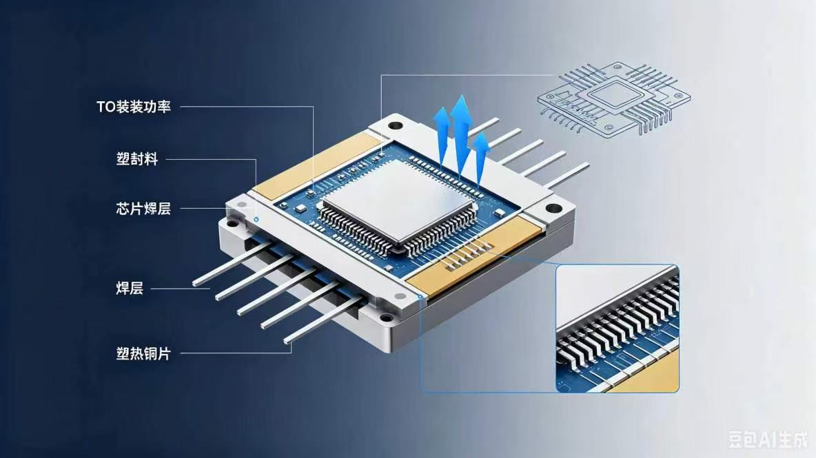
TO packaged power devices are widely adopted in fast charging power supplies, on-board chargers, charging piles, industrial power supplies and other products. The packaging structure is not only responsible for electrical connection, but also serves as the core carrier for heat conduction from the internal chip. Uneven internal solder layers, poor temperature resistance of plastic packaging materials or unqualified pin coplanarity will lead to increased thermal resistance and severe local heat accumulation when devices operate under full load for a long time. Consequently, failures such as plastic delamination, pin cold solder joint and premature aging of components will occur.
The standardized TO packaging process precisely controls the whole workflow including chip bonding precision, solder layer thickness, high-temperature molding and pin surface electroplating to reduce the thermal resistance of components and ensure efficient heat transfer to external heat dissipation structures. Under high-load working conditions such as high-power fast charging, vehicle power supply and 24/7 industrial power supply, packaging quality directly affects the overall temperature rise, operation stability and service life of terminal equipment.
During component selection, thermal resistance, packaging workmanship and batch consistency are equally important as electrical parameters including voltage resistance, rated current and on-resistance. Standardized packaging quality control enables power devices to sustain long-term continuous load operation, and eliminates hidden dangers such as equipment overheating rework and mass failure from the source of materials.