From Wafer to Chip: The Precision Process of Semiconductor Manufacturing
2025-08-20 14:58:51 1160
Semiconductor chips are the core of modern electronic devices, powering everything from smartphones to supercomputers, with nearly all electronic systems relying on these tiny silicon pieces. However, transforming a raw silicon wafer into a powerful chip involves a series of extremely precise manufacturing steps.
-
Wafer Preparation: From Silicon Sand to High-Purity Silicon Wafers
The first step in chip manufacturing is wafer preparation. Wafers are typically made of high-purity monocrystalline silicon, produced through the following process:
-
Silicon Purification: Silicon is extracted from quartz sand (primarily composed of SiO₂) and purified to 99.9999999% (electronic-grade silicon) through chemical processes.
-
Monocrystalline Silicon Growth: Using the Czochralski (CZ) method or Float Zone (FZ) method, polycrystalline silicon is melted and pulled into cylindrical monocrystalline silicon ingots.
-
Wafer Slicing and Polishing: The silicon ingot is sliced into thin wafers approximately 0.5–1 mm thick, which are then precision-polished to ensure an ultra-flat surface for subsequent lithography processes.
Currently, the mainstream wafer size is 300 mm (12 inches), while more advanced 450 mm wafers are still under development to improve production efficiency and reduce costs.
-
Lithography: Patterning Nanoscale Circuits
Lithography is one of the most critical and complex steps in chip manufacturing, determining transistor density and performance. Its core process includes:
-
Photoresist Coating: A uniform layer of photosensitive material (photoresist) is applied to the wafer surface.
-
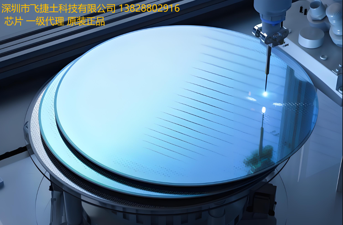
Exposure: A lithography machine (e.g., an EUV extreme ultraviolet lithography machine) projects the designed circuit pattern onto the photoresist, causing chemical reactions in specific areas.
-
Development: Chemical solvents remove the exposed (or unexposed) regions, forming a nanoscale circuit template.
The most advanced EUV lithography technology (13.5 nm wavelength) enables processes at 5 nm and below, while traditional DUV (deep ultraviolet lithography) is used for mature processes (e.g., 28 nm and above).
-
Etching: Sculpting Microstructures
After lithography, etching is used to transfer the pattern onto the silicon wafer. Etching is primarily divided into two types:
-
Dry Etching (Plasma Etching): High-energy plasma bombards the wafer surface to precisely remove silicon material not protected by photoresist.
-
Wet Etching: Chemical liquids (e.g., hydrofluoric acid) dissolve specific materials, suitable for certain specialized structures.
Etching precision directly impacts chip performance, requiring strict control over depth and sidewall morphology.
-
Doping and Ion Implantation
To adjust the conductivity of silicon, impurity atoms (e.g., phosphorus, boron) are implanted into specific regions to form P-type or N-type semiconductors. This process is carried out using ion implantation machines:
-
A high-energy ion beam bombards the wafer surface, altering local electrical properties.
-
High-temperature annealing follows to repair lattice damage and activate the doped atoms.
-
Thin-Film Deposition and Interconnects
Chips require multiple layers of metal interconnects to link transistors. This process involves:
-
Chemical Vapor Deposition (CVD) or Physical Vapor Deposition (PVD): Growing insulating layers (e.g., SiO₂) or metal layers (e.g., copper) on the wafer surface.
-
Electroplating and Chemical Mechanical Polishing (CMP): Copper interconnects are electroplated to fill trenches and then polished flat via CMP to ensure precise alignment of multiple circuit layers.
Modern advanced chips (e.g., 5 nm process) may contain over 10 billion transistors and employ more than 10 layers of metal interconnects.
-
Testing and Dicing
After all processing is completed, the wafer undergoes rigorous testing:
-
Wafer Testing: A probe station checks the electrical performance of each chip, marking defective ones.
-
Dicing: A diamond blade or laser cuts the wafer into individual dies.
-
Packaging: The die is encapsulated in a protective shell and connected to external pins to form the final integrated circuit (IC).
Technical Challenges and Future Trends
As Moore’s Law approaches its physical limits, chip manufacturing faces significant challenges:
-
High Cost of EUV Lithography: An ASML EUV lithography machine costs over $150 million.
-
Quantum Tunneling Effect: Electron leakage may occur at processes below 3 nm, necessitating new materials (e.g., GAA transistors, carbon nanotubes).
-
Advanced Packaging Technologies: Chiplet and 3D stacking are emerging as new directions to enhance performance.
Wafer processing is the core of the semiconductor industry, with a complexity far exceeding that of traditional manufacturing. From silicon sand to high-performance chips, each step embodies cutting-edge technology in materials science, optics, chemistry, and precision engineering. In the future, with advancements in artificial intelligence, 5G, and quantum computing, chip manufacturing will continue to drive technological progress and shape the future of the digital world.